目录
ToggleExploring the Essentials of 2-Layer PCBs: A Comprehensive Guide
Introduction to 2-Layer PCBs
2-Layer PCBs are a fundamental technology in electronics, offering a balanced solution between complexity and cost-effectiveness. These PCBs consist of two conductive copper layers, making them suitable for a wide range of less complex electronic applications where cost and space are considerations.
Designing a 2-Layer PCB
The design process of 2-Layer PCBs involves strategic planning to optimize the placement of components and routing of circuits. Designers must consider factors like signal integrity, power distribution, and electromagnetic interference to ensure the PCB performs reliably. CAD software is utilized to create precise layouts and schematic representations.
Materials Used in 2-Layer PCBs
The choice of materials in a 2-Layer PCB significantly affects its properties and suitability for different applications. Commonly, these PCBs are made with an FR4 substrate, which provides a balance of cost, durability, and electrical performance. The conductive layers are typically copper, known for its excellent electrical conductivity.
Manufacturing Process
The fabrication of a 2-Layer PCB involves several meticulous steps. It starts with the preparation of the base material, followed by applying a protective layer of photoresist. The circuit pattern is then etched onto the board, and holes are drilled for mounting components. The PCB undergoes plating, solder masking, and silkscreening before the final inspection and testing.
Basic Parameters of 2-Layer PCBs
| Parameter | Description |
|---|---|
| Layer Count | 2 |
| Material | Typically FR4 |
| Board Thickness | Commonly 1.6 mm |
| Copper Thickness | 1 oz per square foot as standard |
| Minimum Trace Width | Typically 0.1 mm (4 mil) |
| Minimum Hole Size | Usually 0.3 mm (12 mil) |
| Surface Finish | Options like HASL, ENIG, OSP |
| Solder Mask | Available in various colors |
This table outlines the standard specifications for a typical 2-Layer PCB.
Applications and Use Cases
2-Layer PCBs are versatile and are used in a variety of electronic devices, from simple consumer electronics to more complex systems in automotive and industrial applications. Their cost-effectiveness makes them an ideal choice for many manufacturers.
Conclusion
2-Layer PCBs play a crucial role in the field of electronics. They offer a practical solution for numerous applications, marrying simplicity with efficiency and cost-effectiveness. Their wide range of applications and ease of manufacturing make them a popular choice in the electronics industry.

-
PCB Copper Thickness, Trace Width, and Current Relationship
-
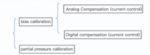
In-depth analysis of chip termination resistance calibration
-
What is the signal propagation delay in PCBs?
-
Unveiling the Secrets of a Six-Layer PCB Stackup: Maximizing Performance and Efficiency
-
Mastering PCB Trace Width Design for Optimal Circuit Performance