OUR PCBS
High Speed PCB
Topfast provides high speed PCB manufacturing services. We utilize automated processes that are capable of handling the most complex board designs with the highest level of accuracy.
You'll like it.
-
Rogers PCB
-
High Frequency PCB
-
High Sepeed PCB
-
2 Layer Board
-
4 Layer Board
High Speed PCB
Characteristics &Manufacturing
Introduction to High Speed PCB
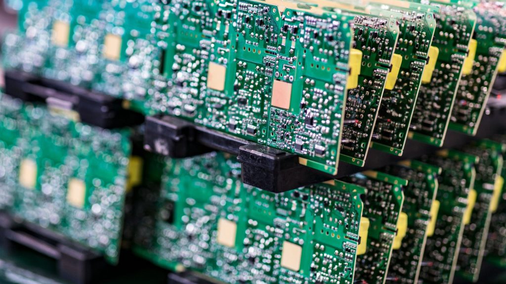
High Speed PCB refers to printed circuit boards specifically designed and manufactured for high-speed data transmission. They are widely used in computer systems, communication equipment, consumer electronics, and data centers. High Speed PCBs offer excellent signal integrity, stability, and reliability, enabling high-speed signal transmission while reducing signal distortion and noise interference to meet the demands of high-speed data communication.
Manufacturing Process of High Speed PCB
-
01
Material Selection
Materials suitable for high-speed applications, such as high-frequency laminates with low dielectric constant and low loss tangent, are chosen. The selection of materials is crucial for signal transmission speed and quality.
-
02
Material Preparation
Selected materials undergo necessary pre-treatments, including impurity removal and control of material thickness and uniformity.
-
03
Special Layer Stackup Design
High Speed PCBs typically employ multilayer structures comprising ground planes, isolation layers, and signal layers. Such layer stackups facilitate good signal isolation, impedance control, and signal integrity.
-
04
Process Control
Parameters such as line width, line spacing, via size, and layer-to-layer spacing are strictly controlled. Accurate control of these parameters is crucial for impedance matching and consistent signal transmission.
-
05
Circuit Fabrication
Circuit patterns are transferred onto the PCB substrate using photolithography techniques, and circuit traces are formed using chemical etching or mechanical milling methods. Special attention is given to meet the fine line width and spacing requirements to achieve precise high-speed signal transmission.
-
06
Drilling and Inner Layer Processing
Drilling and inner layer processes include drilling at appropriate locations and creating microvias and blind/buried vias between inner layers. These vias are used for interconnecting signals and power planes between different layers.
-
07
Surface Treatment
Chemically or metallurgically treating the walls of drilled vias to form reliable conductive layers enhances signal transmission reliability and performance.
-
08
Surface Plating
Protective metals such as nickel and gold are electroplated onto the signal layers and connectors of the PCB to improve conductivity and corrosion resistance.
-
09
Panelization and Processing
The High Speed PCB is cut into the desired shape and size according to design requirements through processes like cutting, drilling, and bending.
-
10
Component Assembly
Electronic components and connectors are mounted on the High Speed PCB using techniques such as soldering or adhesive bonding.
-
11
Testing and Validation
Electrical testing, signal integrity analysis, and validation are performed on the completed High Speed PCBs to ensure they meet the requirements of high-speed data transmission.