目录
ToggleIn-depth analysis of chip termination resistance calibration
(1) Impedance matching on PCBs
(2) On-chip impedance matching
Direct termination of impedance matching and on-chip impedance matching on PCB near the chip can achieve high accuracy and stability, but it needs to occupy a large area, and with the increase of system complexity, impedance matching is used in many places, which requires on-chip de-integration of impedance matching resistors. According to the nature of the resistor itself, it can be divided into passive resistors and active resistors, and this classification belongs to the category of on-chip impedance matching. Passive resistors are usually used in polycrystalline silicon resistors, polycrystalline silicon can be placed directly into the terminal as a matching resistor, polycrystalline silicon has a very good linearity and temperature characteristics, and capacitive loading is small, but to go to the disadvantage of the accuracy is not high. TSMC 65nm process, for example, its accuracy is only 1 ± 30%, but high-speed serial interface to the matching resistor accuracy requirements are very high, so both from the PVT point of view, or from the polycrystalline silicon resistor accuracy itself, need to be accurately calibrated.
The current main calibration methods are divided into the following categories:
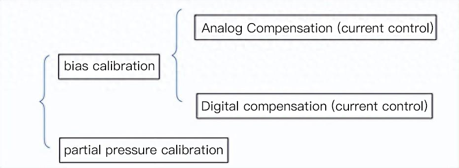
Bias calibration
Bias calibration, mainly through the chip’s internal current mirror to the external precision calibration resistor and internal calibration resistor BLOCK irrigation current, through the resulting bias voltage to regulate the need to calibrate the resistor module, the method of regulation can also be divided into two categories: analog current control and digital voltage control.
Analog current control is through the analog bias voltage control Vgs voltage, and thus control the current flowing through the output driver TRANSISTOR, its defects are very obvious, on the interference and noise is very obvious; while the digital voltage control, is through the voltage to turn on or off the output driver in parallel, the noise has a very good suppression, but also easy to digitize.
I/O termination impedance calibration
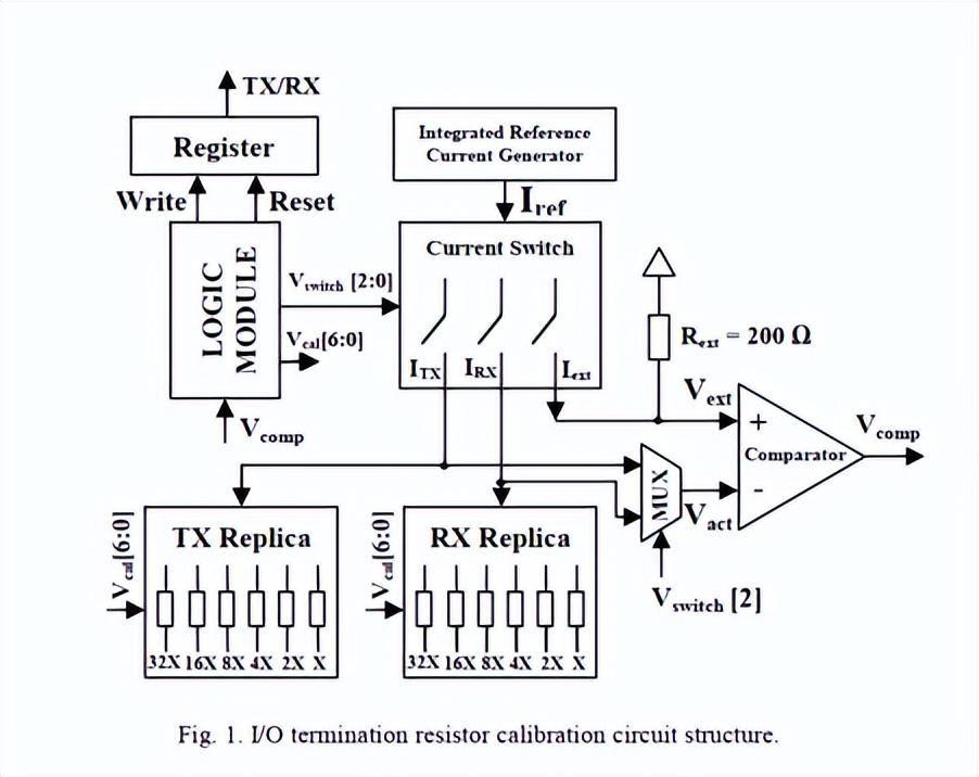
The I/O termination impedance calibration circuit is shown in Figure 1: it consists of two parts, analog and digital, in addition to a high-precision 200ohm resistor external to the chip (it can also be designed for other impedances, e.g., 1.8K, etc.), and an integrated reference current-mirror current source inside the chip (supplying a DC current of 3.25mA), which has three branches that feed the TX, RX, and external REXT calibration resistor, while the switching of each branch is realized by a CMOS transmission gate (TG) (the current mirror currents are assumed to be identical when mismatch is ignored). The detailed current mirror and switching circuit is shown below:
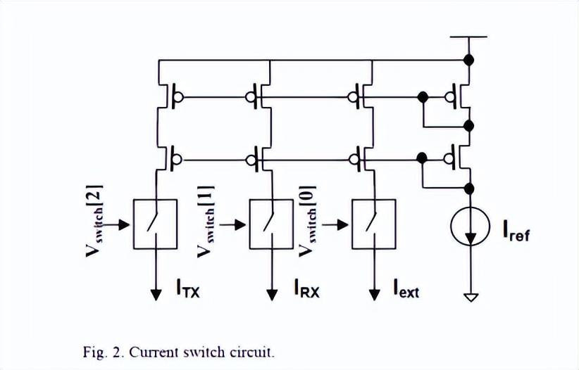
Calibration circuit
Calibration circuit, in fact, the calibration of the TX and RX calibration circuit is replica blocks (later uniformly called replica blocks), the so-called replica, means that the replica is actually TX/RX input/output termination matching circuit, there is a little difference is that the replica blocks need to be calibrated resistance and off-chip precision calibration resistor is not necessarily equal to the replica blocks in this case, the replica blocks of the target calibration resistor value of 200ohm.
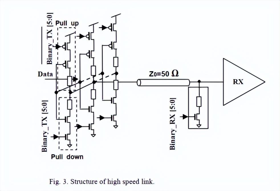
As shown in the figure above, it shows a simple TX to RX link architecture: the TX output is connected to a resistor and an output buffer, the transmission line (50ohm) and the input side of the RX are connected to a resistor module, whereas for a normal interface, there is only 1 buffer for the TX and only one differential op-amp for the RX.
During the calibration process, the TX/RX termination resistor will get the binary calibration code of the replica block from the registers after the calibration circuit has been calibrated, and then set a 50ohm impedance in the TX/RX termination circuit. Since the Makuhari calibration impedance of the duplicate block is four times the termination impedance of the high-speed Link, the 50ohm impedance is generated by processing the TX/RX termination resistor array based on the calibration code.

As shown in the figure above, the replica block circuit, contains GROUPs with different resistance values, each GROUP has resistors in parallel and a control MOS (which can operate in the cutoff or triode region), each resistor can be controlled by the switching of the MOS (using the binary code from the logic block), each GROUP has a resistance value that is twice that of the next, and in this scheme there are seven GROUPs , the first one has the smallest resistance (32X) and the sixth one has only 1 resistance (X).
The binary code of MSB [5] is connected to the smallest resistor GROUP (32X), LSB [5] is then connected to the largest resistor GROUP, and in order to avoid excessive resistance of Rcal, a minimum set of GREOUPs (R=64X) is therefore added.
The calibration circuit provided a constant resistance of 200ohm under various PVT conditions, but usually the resistance variation can range up to ±50ohm, so in a typical case at least a resistance calibration range of 150 to 250ohm is required, and this condition was used to select the resistor values for each replica module.
In the solution proposed in this paper, the normally open GROUP has a resistance value of 300ohm (64X=300ohm), so when the binary code is 0 (Vcal=000000), the total resistance value is 300ohm, and when all GROUPs are open (Vcal=000000), the total resistance value is 150ohm.
For the intermediate input binary code, it is important to have a replica block resistor of around 200ohm in a typical case.
The calibration principle for both TX and RX replication blocks is basically the same, but there is a small difference: the output of the TX is connected to a resistor block that is part of the driver circuitry, and there are two resistors on the pull-up and pull-down paths, the first resistor is used for the data input, and the second resistor is controlled by the binary code of the TX replication block, so for the TX circuit, only the pull-down circuit is used in the replication block and after the calibration is done, the binary code is also used in the TX pull-up circuit. In fact, the TX replication fast each resistor can be represented as two NMOS tubes plus a resistor in series as shown below:

The first transitor receives the binary code, the second transistor is pulled high and is normally open, and the single resistor block of the RX replication module is represented as an NMOS transistor (binary input) and resistor connected in series.
The I/O termination resistor calibration circuit has the following components:
(1) Logic control module;
(2) Multiplexer;
(3) Comparator;
The logic control module is used to provide all the digital signals such as calibration code (Vcal), switching signals (Vswitch) for controlling the current switches, multiplexer, and reset signals to write the data/reset register (the register is used to save the calibration code), the comparator is used to compare the calibration voltage of the replica block with the external reference voltage, and the output voltage (Vcomp) is used as the logic module’s Input.

The calibration process is shown in the table above, starting from RX, a 3-bit signal (generated by the logic module), which is used to control the current switch, cuts to the RX mode (which means that no current passes through the TX replica block), the current passes through the RX replica block and the external calibration resistor, and the Vswitch signal, which will control the multiplexer and turn its path on.
The Vswitch signal will control the multiplexer and open its path to send the voltage of the RX replica block to the comparator; in the next stage the logic control module, starts to increase the 6-bit calibration code (Vcal) and change the impedance of the RX replica block, the precise calibration depends on the calibration bit (the more bits, the more precise the calibration), the calibration of the replica block will be started from the highest value (vcal=000000), the resistance of replica block at this time is about 300ohm, at the end of the calibration, the replica block will have the lowest resistance value because all the resistor blocks are open and in parallel (Vcal=111111). The resistance value will also fall to 150ohm and the calibration STEP will have 63 steps.
Nstep=2^n-1
Vext is the positive phase input to the calibration resistor (the external voltage drop is 200*Iref), the current of the RX replica module is also constant (equal to Iref), but its actual impedance is decreasing during the calibration period, so the voltage drop of the RX replica block is also decreasing, and at the same time, when the replica block’s voltage drop reaches the external reference voltage (Vact=Vext), the output of the comparator will be cut from 0 to 1 ( Vcomp=1), at this point the logic module will stop decreasing the calibration code (Vcal) and store a fixed calibration code in the register, this calibration code will be transferred from the register to the real input termination module providing a fixed 50ohm resistance (1/4 of the RX replica block).