OUR PCBS
HDI PCB
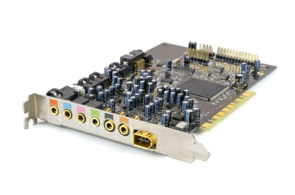
Topfast provide comprehensive High-Density Interconnect (HDI) PCB manufacturing services. Our specialized equipment and highly trained technicians fabricate HDI PCBs with exceptional complexity, accuracy, and precision.
You'll like it.
-
Rogers PCB
-
High Frequency PCB
-
High Sepeed PCB
-
2 Layer Board
-
4 Layer Board
HDI PCB
Characteristics &Manufacturing
Introduction to HDI PCB
HDI PCB, which stands for High-Density Interconnect Printed Circuit Board, is an advanced technology used in PCB design to achieve higher circuit density, smaller form factor, and improved performance. HDI PCBs find extensive applications in various industries, including mobile communication, computing, consumer electronics, medical devices, and automotive electronics. They provide essential solutions for miniaturization, high-speed signal transmission, and complex functionality in modern electronic devices.
Manufacturing Process of HDI PCB
-
01
Material Preparation
High-quality materials suitable for HDI PCB production, including substrates, copper foils, and coverlay materials, are selected. The quality and performance of these materials are critical for the final product's quality and reliability.
-
02
Inner Layer Fabrication
The inner layer structure is formed by laminating the substrate and copper foils together. Thin-core substrates and microfine line patterning techniques are commonly employed to achieve high-density interconnects in the inner layers.
-
03
Microvia Drilling
Microvias and blind/buried vias are drilled on the inner layers. These microvias serve as interconnections between different layers, enabling high-density routing.
-
04
Surface Treatment
Through chemical or metallization processes, reliable conductive layers are formed on the walls of drilled microvias, enhancing signal transmission reliability and performance.
-
05
Outer Layer Fabrication
The outer layer structure is added on top of the inner layers, and outer circuitry is formed through processes like etching or copper plating.
-
06
Patterning
Photolithography techniques are used to transfer the circuit pattern onto the outer layer copper foil, defining the desired wire routing and interconnections.
-
07
Surface Finishing
Protective metals, such as nickel and gold, are electroplated onto the circuitry of the outer layers. This enhances conductivity and corrosion resistance.
-
08
Panelization and Processing
The HDI PCB is cut into the desired shape and size through processes like cutting, drilling, and bending, according to the design requirements.
-
09
Component Assembly
Electronic components and connectors are mounted onto the HDI PCB using techniques like soldering or bonding.
-
10
Testing and Inspection
The completed HDI PCBs undergo electrical testing, signal integrity analysis, and reliability inspections to ensure compliance with specifications.
-
11
Packaging and Delivery
The finished HDI PCBs are packaged according to customer requirements and delivered accordingly.