OUR PCBS
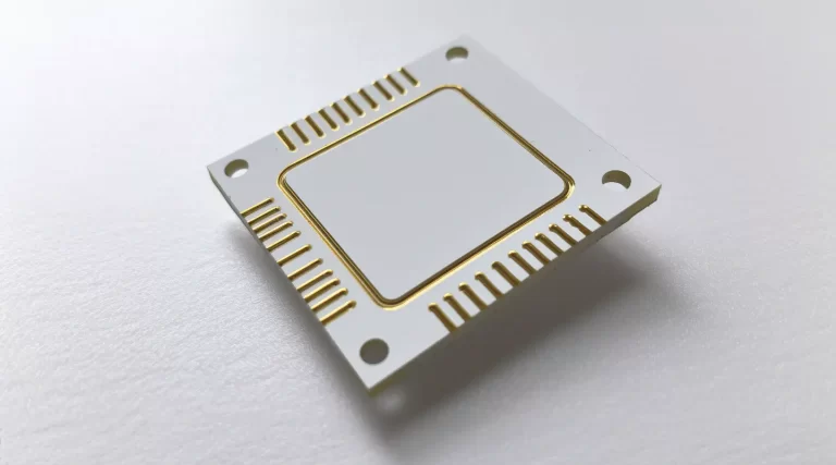
Ceramic PCB
Topfast manufactures ceramic printed circuit boards (PCBs) that provide superior electrical and thermal performance. Our ceramic PCBs feature excellent insulation, fast heat dissipation and stable shape.
You'll like it.
-
Rogers PCB
-
High Frequency PCB
-
High Sepeed PCB
-
2 Layer Board
-
4 Layer Board
Ceramic PCB
Characteristics &Manufacturing
Introduction to Ceramic PCB
Ceramic PCB, also known as Ceramic-based PCB or Ceramic Substrate PCB, is a type of printed circuit board that utilizes ceramic material as the substrate. Ceramic PCBs offer excellent high-temperature stability, superior insulation properties, and good resistance to chemical corrosion. They are commonly used in high-power electronic devices, RF circuits, and high-frequency applications. Ceramic PCBs effectively handle high-temperature environments, high-frequency signals, and complex circuit requirements, delivering exceptional performance and reliability.
Manufacturing Process of Ceramic PCB
-
01
Ceramic Material Selection
Suitable ceramic materials for Ceramic PCBs are chosen, commonly including alumina (Al2O3) and aluminum nitride (AlN). Material selection depends on factors such as high-temperature stability, insulation properties, and thermal conductivity.
-
02
Material Preparation
Pre-processing is performed on the selected ceramic materials, including cleaning, grinding, and applying protective coatings. This ensures surface smoothness and cleanliness of the material.
-
03
Substrate Preparation
The ceramic material is cut into the desired dimensions and shapes. Mechanical cutting or CNC cutting methods are typically employed.
-
04
Ceramic Material Sintering
The ceramic substrate undergoes high-temperature sintering to achieve the desired physical and chemical properties. This step is usually carried out in a high-temperature furnace.
-
05
Pattern Formation
Circuit patterns are transferred onto the ceramic substrate surface using photolithography techniques. This involves applying photoresist, exposure, and development steps to form the circuit patterns.
-
06
Metallization
A metal layer is coated onto the ceramic substrate, often using high-temperature sintering or pressing methods to convert metal powders into a conductive layer.
-
07
Metal Plating
The metallized layer is subjected to metal plating to enhance conductivity and corrosion resistance. Common plating methods include nickel (Ni), gold (Au), tin (Sn), among others.
-
08
Surface Treatment
Surface treatment is performed on the ceramic substrate, including cleaning, coating protective layers, and polishing, to enhance appearance and durability.
-
09
Component Assembly
Electronic components are mounted on the Ceramic PCB using soldering or surface mounting techniques.
-
10
Soldering
Suitable soldering methods, such as surface mount technology (SMT) or through-hole soldering, are employed to connect electronic components to the Ceramic PCB.
-
11
Testing and Validation
Electrical testing and performance validation are conducted on the completed Ceramic PCB to ensure it meets design requirements and application needs.