目录
TogglePCB Copper Thickness, Trace Width, and Current Relationship
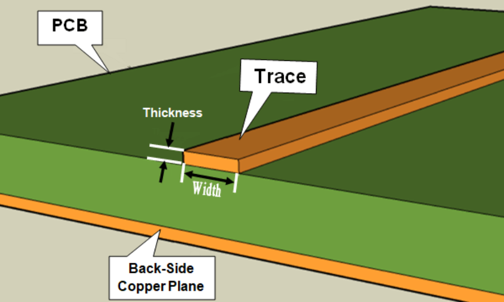
The capacity of a PCB to carry current is influenced by various factors, including trace width, copper thickness, and permissible temperature rise. Generally, wider traces can handle more current. However, it’s essential to understand the precise relationship between trace width, copper thickness, and current-carrying capacity for effective PCB design.
1.PCB Current and Trace Width:
The ability of a PCB to carry current is directly related to trace width, copper thickness, and allowable temperature rise. Wider traces typically have higher current-carrying capacities. However, the relationship between trace width and current capacity is not linear. International standards provide valuable data on this relationship, helping designers determine the appropriate trace width for specific current requirements.
2.PCB Copper Thickness, Trace Width, and Current Relationship:
Before exploring the relationship between copper thickness, trace width, and current, it’s crucial to understand the units used to express PCB copper thickness: ounces, inches, and millimeters. Typically, copper thickness is expressed in ounces per square inch (oz/sq.in), with common conversions to inches and millimeters provided for reference.
Additionally, empirical formulas can be used to calculate the relationship between trace width (W) and current-carrying capacity (A), offering practical guidance for PCB design. These formulas take into account factors such as temperature rise and copper thickness to ensure reliable performance.
copper thickness/35um | copper thickness/50um | copper thickness/70um | |||
amps(A) | line width(mm) | amps(A) | line width(mm) | amps(A) | line width(mm) |
4.5 | 2.5 | 5.1 | 2.5 | 6 | 2.5 |
4 | 2 | 4.3 | 2.5 | 5.1 | 2 |
3.2 | 1.5 | 3.5 | 1.5 | 4.2 | 1.5 |
2.7 | 1.2 | 3 | 1.2 | 3.6 | 1.2 |
2.3 | 1 | 2.6 | 1 | 3.2 | 1 |
2 | 0.8 | 2.4 | 0.8 | 2.8 | 0.8 |
1.6 | 0.6 | 1.9 | 0.6 | 2.3 | 0.6 |
1.35 | 0.5 | 1.7 | 0.5 | 2 | 0.5 |
1.1 | 0.4 | 1.35 | 0.4 | 1.7 | 0.4 |
0.8 | 0.3 | 1.1 | 0.3 | 1.3 | 0.3 |
0.55 | 0.2 | 0.7 | 0.2 | 0.9 | 0.2 |
0.2 | 0.15 | 0.5 | 0.15 | 0.7 | 0.15 |
PCB design copper-platinum thickness, line width and current relationship table
3.PCB Design Considerations:
When designing PCBs, it’s essential to consider factors beyond trace width and copper thickness. The number of components, solder pads, and vias can also affect current-carrying capacity. Additionally, the presence of solder pads and vias can significantly impact the current distribution along the traces. Careful design considerations, such as distributing current evenly and managing temperature rise, are crucial for optimal performance.

4.Experience-Based Guidelines:
Experience-based guidelines provide valuable insights into designing PCB traces to safely carry current. For example, a commonly accepted rule suggests that traces with a cross-sectional area of 1 square millimeter can safely carry 10A of current. This guideline helps designers avoid overheating and trace failure due to excessive current flow.

Conclusion:
In conclusion, understanding the relationship between trace width, copper thickness, and current is essential for effective PCB design. By considering factors such as temperature rise, component density, and empirical guidelines, designers can create PCB layouts that meet performance requirements and ensure reliability in various operating conditions.