目录
ToggleUnveiling the Secrets of a Six-Layer PCB Stackup: Maximizing Performance and Efficiency
When it comes to PCB design, the stackup plays a crucial role in determining the overall performance and efficiency of the circuit board. A well-designed stackup ensures signal integrity, impedance control, and thermal management, among other factors. By understanding the intricacies of PCB stackup, designers can unlock the full potential of their six-layer PCBs.
Fundamentals of Six-Layer PCB Stackup Design
In the realm of PCB design, the stackup configuration is akin to the foundation of a building, providing structural integrity and support for the entire system. A well-designed stackup not only facilitates the interconnection of components but also plays a pivotal role in ensuring signal integrity, impedance control, and thermal dissipation. Let’s delve into the fundamental principles of six-layer PCB stackup design and explore key considerations for optimizing performance and efficiency.
1.1 Understanding the Layer Structure
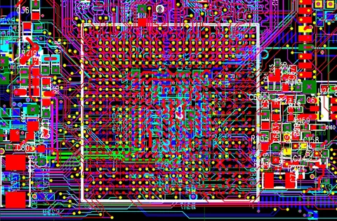
A typical six-layer PCB stackup comprises alternating layers of signal traces, ground planes, and power planes, sandwiched between insulating dielectric layers. The arrangement of these layers significantly impacts signal propagation, electromagnetic interference (EMI) mitigation, and thermal characteristics. Designers must carefully plan the layer structure to achieve optimal performance.

1.2 Signal Routing and Layer Allocation
Effective signal routing is paramount to ensure signal integrity and minimize crosstalk between adjacent traces. By allocating specific layers for signal traces and maintaining appropriate spacing between them, designers can mitigate signal distortion and improve overall system reliability. Proper layer allocation also facilitates impedance matching and reduces transmission line effects.
1.3 Ground and Power Plane Considerations
Ground and power planes serve as critical elements in the PCB stackup, providing stable reference planes for signal return paths and supplying power to active components. Careful placement and distribution of ground and power planes help minimize noise coupling, reduce ground loops, and enhance EMC performance. Ensuring adequate decoupling capacitance between power and ground planes is essential for suppressing voltage fluctuations and maintaining signal integrity.

1.4 Impedance Control and Signal Integrity
Maintaining consistent impedance levels throughout the PCB stackup is vital for high-speed digital and RF applications. By controlling trace widths, layer thicknesses, and dielectric properties, designers can achieve precise impedance matching and minimize signal reflections. Advanced impedance calculation techniques, such as controlled impedance routing and differential pair routing, play a crucial role in ensuring signal integrity and system reliability.

1.5 Thermal Management Strategies
Efficient thermal management is essential to prevent overheating of electronic components and ensure long-term reliability. By incorporating thermal vias, heat sinks, and copper pours into the PCB stackup, designers can effectively dissipate heat and maintain optimal operating temperatures. Proper component placement and thermal relief design further enhance heat dissipation and prevent thermal hotspots.
1.6 Conclusion
In summary, mastering the fundamentals of six-layer PCB stackup design is essential for achieving optimal performance and efficiency in electronic systems. By understanding the layer structure, optimizing signal routing, and implementing effective ground and power plane strategies, designers can create robust PCB designs that meet the most demanding application requirements.
Understanding Layer Arrangement
When designing a six-layer PCB stackup, understanding the layer arrangement is crucial. Typically, a six-layer stackup consists of signal layers, power planes, and ground planes strategically arranged to optimize performance and efficiency.
1. Signal Layers:
The signal layers, usually located in the center of the stackup, carry the electrical signals between components. These layers require careful planning to avoid signal interference and ensure signal integrity.

2. Power Planes:
In a six-layer stackup, there are usually two power planes, one for supplying power and the other for distributing power to the components. Proper placement and routing of power planes are essential to minimize power losses and ensure stable voltage regulation.
3. Ground Planes:
Similar to power planes, there are typically two ground planes in a six-layer stackup. Ground planes serve as return paths for electrical currents and help reduce electromagnetic interference (EMI) and noise in the circuit. Proper grounding techniques are crucial for maintaining signal integrity and reducing noise.
4. Layer Arrangement Considerations:
When arranging the layers in a six-layer PCB stackup, several factors need to be considered, including signal integrity, power distribution, thermal management, and EMI/EMC requirements. Careful planning and simulation tools are often used to optimize the layer arrangement for the specific application requirements.
5. Layer Stacking Order:
The order in which the layers are stacked can significantly impact the performance of the PCB. Common stacking orders include signal-power-signal-ground-ground-signal (SPSGGS) and signal-ground-power-ground-signal-signal (SGPGSS), among others. The choice of stacking order depends on factors such as signal integrity, power distribution, and thermal management needs.
6. Thermal Considerations:
Proper thermal management is essential in a six-layer PCB stackup to ensure the components operate within their specified temperature range. This involves strategically placing thermal vias, thermal pads, and copper pours to dissipate heat effectively and prevent overheating.
7. Simulation and Analysis:
Before finalizing the layer arrangement, it is crucial to perform simulations and analysis using specialized software tools. This helps identify and mitigate potential issues related to signal integrity, power distribution, thermal management, and EMI/EMC compliance.
Optimizing Signal Integrity
Signal integrity is paramount in a six-layer PCB stackup to ensure reliable communication between components and prevent signal degradation. This section explores various strategies to optimize signal integrity in a six-layer PCB stackup.
1. Impedance Control:
Maintaining consistent impedance throughout the PCB traces is critical for signal integrity. Impedance mismatches can lead to signal reflections, ringing, and signal integrity issues. By carefully designing trace widths, spacing, and layer stackup, designers can achieve the desired impedance values for high-speed signals.
2. Differential Pair Routing:
Differential pairs are commonly used for high-speed signaling to minimize electromagnetic interference (EMI) and crosstalk. Proper routing techniques, such as controlled impedance routing and length matching, are essential to maintain signal integrity and minimize skew between differential pairs.
3. Via Placement and Design:
Vias play a crucial role in signal integrity by providing a path for signals to transition between different layers. Proper via placement and design, including via stitching, via shielding, and via fanout, are essential to minimize signal distortion and maintain impedance continuity.
4. Crosstalk Mitigation:
Crosstalk occurs when signals from adjacent traces interfere with each other, leading to signal distortion and integrity issues. Techniques such as increasing trace spacing, using ground planes between signal layers, and implementing shielding techniques can help mitigate crosstalk and improve signal integrity.
5. Return Path Design:
Ensuring a low-impedance return path for signals is essential to prevent signal distortion and maintain signal integrity. Ground planes and power planes should be carefully designed to provide a clear return path for signals and minimize ground bounce and noise.
6. High-Speed Design Guidelines:
Following high-speed design guidelines, such as minimizing signal traces length, reducing discontinuities in signal paths, and optimizing termination schemes, is crucial for achieving optimal signal integrity in a six-layer PCB stackup.
7. Simulation and Validation:
Before finalizing the PCB design, it is essential to perform signal integrity simulations and validation using specialized software tools. This helps identify and mitigate potential signal integrity issues early in the design process, ensuring robust performance in the final product.