OUR PCBS
High Frequency PCB
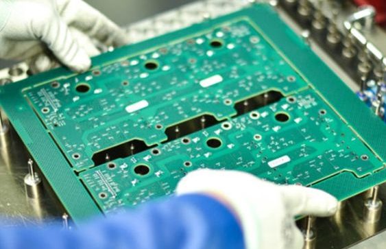
Topfast provides high-frequency PCB manufacturing. We use advanced machines and materials to ensure a precise and reliable end product. Our strict quality standards ensure that all of our PCBs are built to perform.
You'll like it.
-
Rogers PCB
-
High Frequency PCB
-
High Sepeed PCB
-
2 Layer Board
-
4 Layer Board
High Frequency PCB
Characteristics &Manufacturing
Introduction to High Frequency PCB
High Frequency PCB, also known as RF PCB (Radio Frequency PCB), is a type of printed circuit board specifically designed and manufactured for high-frequency signal transmission and RF applications. They find extensive use in wireless communications, radar systems, satellite communications, aerospace, medical devices, and high-speed data transmission. High Frequency PCBs are characterized by low transmission loss, low signal distortion, strict impedance control, and effective electromagnetic shielding. They employ specific materials and design techniques to meet the requirements of high-frequency signal transmission.
Manufacturing Process of High Frequency PCB
-
01
Material Selection
Suitable materials for high-frequency applications, such as PTFE (Polytetrafluoroethylene) and RF-PTFE (RF Glass Reinforced Polymer), with low dielectric constant and low loss tangent, are chosen. The quality and performance of these materials significantly impact the transmission loss and signal speed of the High Frequency PCB.
-
02
Material Preparation
The selected materials undergo necessary pre-treatments, such as impurity removal and control of material thickness and uniformity.
-
03
Special Layer Stackup Design
High Frequency PCBs often have multi-layer structures comprising ground planes, isolation layers, and signal layers. This layer stackup aids in achieving signal isolation, impedance control, and electromagnetic shielding.
-
04
Process Control
Strict control of parameters like line width, line spacing, via size, and layer-to-layer spacing is crucial. Accurate control of these parameters ensures impedance matching and consistent signal transmission.
-
05
Circuit Fabrication
The circuit pattern is transferred onto the PCB substrate using photolithography techniques. Processes like chemical etching or mechanical machining are used to create circuit traces. Attention is paid to meet the fine line width and spacing requirements for precise high-frequency signal transmission.
-
06
Drilling and Inner Layer Processing
Drilling is performed at specific locations, and microvias and blind/buried vias are created between the inner layers. These vias serve to interconnect different layers and achieve impedance matching and signal transmission.
-
07
Surface Treatment
The drilled vias' walls are treated chemically or metallurgically to form reliable conductive layers, improving the reliability and performance of signal transmission.
-
08
Surface Plating
Protective metals, such as nickel and gold, are electroplated onto the signal layers and connectors to enhance conductivity and corrosion resistance.
-
09
Panelization and Processing
The High Frequency PCB is cut into the desired shape and size through processes like cutting, drilling, and bending, according to the design requirements.
-
10
Component Assembly
Electronic components and connectors are mounted on the High Frequency PCB using techniques like soldering or adhesive bonding.
-
11
Testing and Validation
The completed High Frequency PCBs undergo electrical testing, signal integrity analysis, and validation to ensure they meet the requirements of high-frequency signal transmission.