目录
ToggleWhat is the signal propagation delay in PCBs?
What is propagation delay on a PCB?
The propagation delay on a PCB trace signal is the unidirectional (source-to-load) time required for transmission over that alignment. It is expressed as a unit length of time. Propagation delay is a function of dielectric constant (Er) and trace geometry. For a given PCB laminate and a given dielectric constant, the delay is fixed for different impedance traces. Learn moreRead how to select PCB materials and laminates .
Why do propagation delays occur?
Stray capacitance is the cause of delay in any circuit. We don’t intentionally use capacitors in our circuits; however, there are still capacitors. The total capacitance depends on their relative size and the geometry of the traces. Stray capacitances include the capacitance between lines, the capacitance between a line and an adjacent ground plane, and the capacitance between the trace and free space.
The effect of stray capacitance results in signal delay. The bottom line is that when a digital signal changes state, it takes some time for the transition to take place at the destination due to the stray capacitance that must be charged and discharged.
Leave your contact details : Get free High Speed PCB Design Guide :

What is the difference between transmission delay and latency?
Transmission delay and propagation delay can be used interchangeably, but they need to be treated differently when the system needs to be analyzed from the analog/digital side.
Timing of logic signals in a PCB alignment can be calculated by the following transmission line method:
Method 1: Terminate the transmission line by its characteristic impedance when the delay on one side of the PCB alignment is equal to or greater than half the rise/fall time of the applied signal.
Example: a 2-inch microstrip line with an Er of 4 will exhibit a delay of approximately 270 ps. Using the above method, the termination will be accurate when the signal rise time is less than 500ps.
Method 2: Use the PCB alignment length 2 inch/ns (rise/fall time) method. If the signal alignment exceeds the alignment length criteria, termination must be used.
Example: A PCB alignment designed for high-speed logic with a rise/fall time of 5ns should be terminated by its characteristic impedance if the alignment length is equal to or greater than 10 inches.
How does propagation delay affect the speed of signals on PCB alignments?
When PCBs operate at high frequencies, their alignment paths need to be treated as transmission lines. Controlled impedance calculations are important for these transmission lines so that signal reflections, crosstalk, noise and ground bounce may be mitigated. These issues require special attention because they can pose a threat to signal quality, which can lead to failure of the entire system. This is why we need to know the speed at which a signal travels through a transmission line and the propagation delay associated with it.
How to calculate the signal speed?
Electromagnetic signals propagate in a vacuum/air at the same speed as light, i.e:
Vc= 3 x 10^8m/s = 186,000 mils/s = 11.8in/ns
For microstrip/ribbonline PCB designs, the signal velocity is calculated as follows:
Where Vc is the speed of light in vacuum/air.
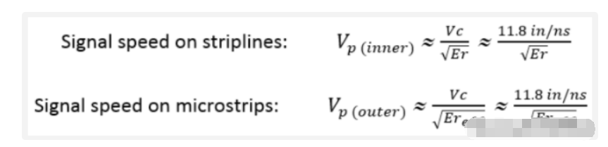
Signal speed in microstrip/strip line PCB design.
Ereff is the effective dielectric constant of a microstrip line and its value is between 1 and Er.
Ereff= (0.64 Er + 0.36)
It indicates if the signal velocity on the PCB is lower than the signal velocity in air. If the PCB material has an Er of 4, then the signal velocity on the stripline design is half that in air, about 6 in/ns.
How to measure propagation delay?
Let’s calculate the propagation delay/time delay using the alignment length and vice versa. Mathematically, the delay is tpd:1/v . Where v is the speed of the signal in the PCB transmission line. In vacuum/air, it is equal to 85 ps/In.
On a PCB transmission line, tpd is given by the following equation:
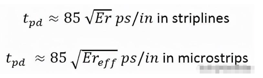
Propagation delay in microstrip/ribbonline PCB design.
The speed of the signal on the interconnect
When a voltage is applied between the signal and return path of a transmission line, the signal travels down the line. There is always a voltage distribution between the signal and the loop. The voltage distribution on a transmission line is shown below.
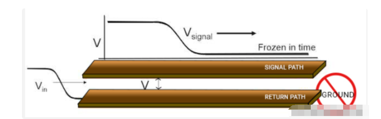
Voltage distribution between signals and loops on a transmission line.
How can propagation delays be reduced/controlled?
We cannot change the speed of the clock signal, but we can change the time of arrival of the signal by changing the PCB trace length. Small changes in trace length can help PCB components to synchronize with the clock signal at the same time to get their fixed state.
Calculation of clock deviation of different PCB components also helps in compensating the propagation delay/time delay problem. Serpentine is another method that provides the signal the required time to reach full level before the next clock pulse arrives. It provides clock pulses that are just the perfect amount of delay. In best practice, it is best to bend differential alignments together and they must remain tightly coupled. So how do you decide which traces must be serpentine?
Determine the longest signal alignment and snake the remaining traces through the network to synchronize signals across all alignments.
Adjust the length of the clock trace that connects the components in a given network.
Delay the clock pulses until the IC can rise to full voltage application.
Note: In a signaling network, an alignment with a mismatched length always matches the alignment with the maximum length. Add curves to shorter traces in order to increase their length.
Alignment Length Adjustment/Matching
Due to timing mismatches, signals traveling through different alignments in the PCB reach the load at different times. Delayed tuning is critical to ensure that data reaches the load at the exact time of the alignment and clock signals in multiple parallel interconnects, differential pairs. Perform alignment length adjustments to address signal delay times.
Delay and alignment length tuning reflect the same idea. For length adjustment, you can set the length of the signaling alignment in matching network groups. As we all know, timing delays are unavoidable. We can only take measures to control it. By placing alignments with the same length in matching groups, we try to ensure that all signals crossing these alignments arrive within a fixed time delay. Now the question is, what if there are two mismatched signal alignments in a match group? It is possible to synchronize signals crossing such alignments by adding delays to the shorter signal traces (called snakes).
In theory, the receiver will immediately receive any waveform/signal sent by ****. We also assume that the clock signals have zero time gap and are processed simultaneously at the receiver. But reality is different. If there is a slight mismatch in the lengths of the PCB alignments, the signals may not arrive at the receiver pins at the same time. PCB alignment tuning ensures that the critical signals arrive at the time of the matching alignments of equal length.
Controlling transmission delay with controlled impedance traces
Different trace geometries/structures are available for controlled impedance traces. The trace configurations we discuss here are based on IPC standard 2141A .
Microstrip line: it consists of a discrete insulated wire separated by a fixed distance on the ground plane. The dielectric can be the insulating wall of the wire or a combination of this insulation and air.
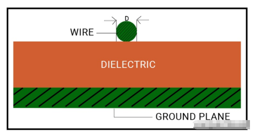
Microstrip wire is a discrete insulated wire separated by a fixed distance in the ground plane.
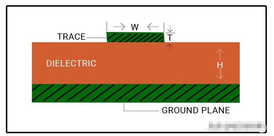
Surface Microstrip: In a double-sided PCB design with a ground layer on one side, the signal trace on the other side can be designed with a controlled impedance. This trace structure is known as surface microstrip or simply microstrip.
One side is a grounding plate and the other side is a surface microstrip line for signal traces.
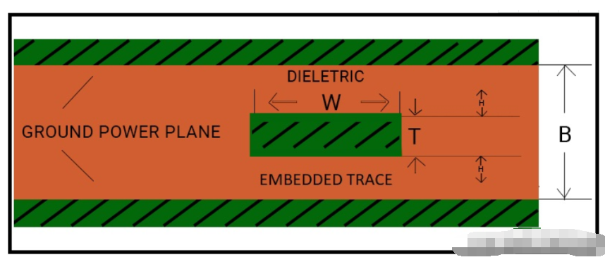
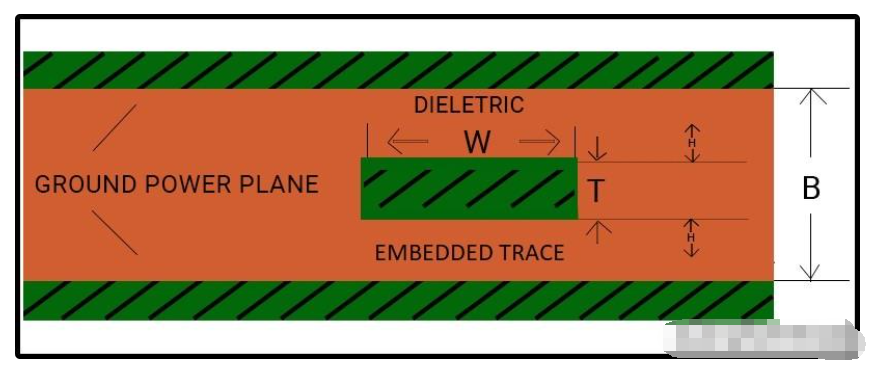
Embedded/Symmetrical Ribbon Lines: In multilayer PCBs, this arrangement realizes signal traces between the power and ground layers. The return current paths of the high-frequency signal traces are located above and below the in-plane signal traces. As a result, the high-frequency signals are retained inside the PCB, thereby reducing **** and shielding other stray signals.
Symmetrical strip lines enable signal tracking between the power and ground planes.
Note: The grounding layer is zero potential, and the low-impedance reference plane is large.
Coplanar structure: Coplanar waveguide structures have a signal track and a return path conductor on the same layer of the PCB. The signal track is located in the center, surrounded by two adjacent outer ground layers; it is called “coplanar” because the three planar structures are located in the same plane, and the PCB dielectric is located underneath. Both microstrip and stripline may have coplanar structures.
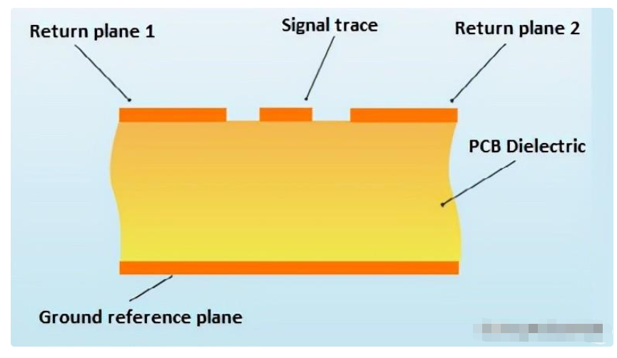
The coplanar structure has a signal track surrounded by two adjacent external strata.
High-Speed PCB Design Rules for Reducing Transmission Delay
Accurate time delay management requires trace length calculations to achieve high speed PCB routing Therefore. the distances between components on the PCB are short. We don’t even consider the time it takes for the signal to travel across the PCB. But in high-speed printed circuit boards. exchanges occur at an edge rate of less than 1 ns. such short distances between components are clearly of paramount importance if you want your system to operate without interference.
The designer must know the specific timing tolerances of the expected PCB signaling.
Different interfaces operating at different data rates using different signaling standards. Specify different allowable lengths or timing mismatches. When planning I/O channels in a PCB, the designer should look for acceptable length mismatches and convert them to allowable timing mismatches.
Avoid substrates with large dielectric constants: Typically, substrates with large dielectric constants result in lower signal velocities, which exceed the allowable specified propagation delays, especially between data lines and clocks.
Concern about pin package delay: when a signal reaches the pins/pad of a specific component, it still needs to cross the exposed conductor path along the inside of the component package. As it traverses the signal traces and connections associated with the internal circuitry, the signal experiences parasitic inductance and capacitance that affects the speed at which the signal travels through the connections compared to the traces. Connecting wires also come in different geometries, increasing the signal delay on different pins/pads. It is recommended to ask the manufacturer for the pin package delay associated with a particular component. It is expressed in picoseconds (ps) or millimeters/microns in length. This length should be considered when performing any delay/length tuning on differential pair signals or single-ended signals.
Watch your “clock skew”: when the length of the clock and the signal trace are different, this can lead to a timing mismatch called clock skew. Ignoring this issue may result in locking the wrong data. The clock delay should be greater than the maximum delay in the data signal.
Check Tilt Duration: For clock and receiver datasheets, always refer to the datasheet for component settings and tolerances.
Material dispersion is a high frequency phenomenon. Always consider the switching frequency.
Before choosing a high-speed PCB design software, consider these parameters
If you are using software that only considers length mismatch, then you can easily calculate the correct length mismatch value for a given substrate. This length mismatch is equal to the timing mismatch multiplied by the signal velocity (in/ns) in the given substrate. A good PCB design software should provide the following for the target propagation delay:
Interactive routing capabilities
Intelligent length adjustment
IPP enhancements (instant access to new and existing features)
Dynamic data modeling (accelerated network list creation)
User-friendly
High-speed printed circuit board materials
As we all know, the signal velocity is not only affected by the trace geometry and trace position, but also by the substrate material. The dielectric constant of the trace determines its signal velocity. Let’s look at an example; if we hang a trace in a vacuum, only the dielectric constant of that trace will affect the speed. If the trace is on the surface of a PCB, the signal velocity is also affected by other nearby dielectrics; this is what happens in a PCB. The trace runs on the PCB substrate material (which has a fixed value of dielectric constant). The dielectric constant of the substrate, the air and the solder mask are the main determinants of the signal speed. This is known as the effective dielectric constant (erbium effective). Board thickness also affects the speed of the signal. View more information to learn about high speed PCB design .
FR4 can be used in high-speed PCB design when layers are laminated with high-speed laminates such as Rogers. in the higher frequency bands FR4 experiences dispersion which increases transmission speeds and reduces transmission delays. electromagnetic absorption in FR4 produces more signal attenuation associated with the traces. For this reason, high-speed laminates are used underneath high-speed traces along with FR4 laminates, especially at frequencies above 5 GHz.
Propagation delay of several PCB materials
The signal speed and propagation/delay of some PCB materials are shown in the table below:

Signal loss versus frequency
The graph below depicts that there is a direct correlation between signal loss and frequency. Also, we can see that certain materials have less loss than others. This graph shows which materials may have better electrical properties at higher speeds.

As frequency increases, some materials exhibit less lossy behavior.
The main function of a printed circuit board is to transmit signals between devices accurately and without loss. Propagation delay or time delay plays an important role in the proper functioning of high speed boards. It cannot be completely avoided, but it can be minimized by using different trace configurations and then matching and bending the lengths as precisely as needed. You should know in your design, the material dielectrics, and which traces require delay measurements. You also need to understand the relationship between signals such as clock and data in order for the board to function properly.
*Blog content for netizens personal release, only on behalf of the blogger's personal views, if any infringement, please contact the staff to delete.