目录
ToggleMastering PCB Trace Width Design for Optimal Circuit Performance
Introduction:
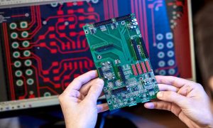
In modern electronics, PCB trace width plays a critical role in determining the performance and reliability of electronic circuits. This article explores the intricate aspects of PCB trace width design and offers valuable insights for engineers and PCB designers striving to achieve optimal circuit performance.
The Fundamentals of PCB Trace Width Design:
PCB trace width directly influences various aspects of circuit performance, including current-carrying capacity, signal integrity, and thermal management. Understanding the fundamentals of trace width design is essential for designing reliable and efficient PCBs.
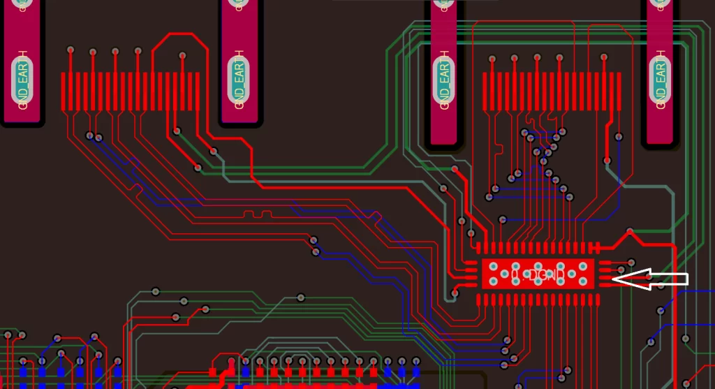
Image source: Images are sourced from the internet. If there are any copyright concerns, please contact us for removal. Thank you.
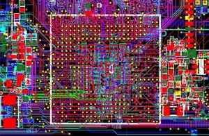
Factors Influencing PCB Trace Width:
Several factors must be considered when determining the appropriate trace width for a PCB design. These include the maximum current requirements, acceptable voltage drop, operating temperature, and the dielectric properties of the PCB substrate.

Image source: Images are sourced from the internet. If there are any copyright concerns, please contact us for removal. Thank you.
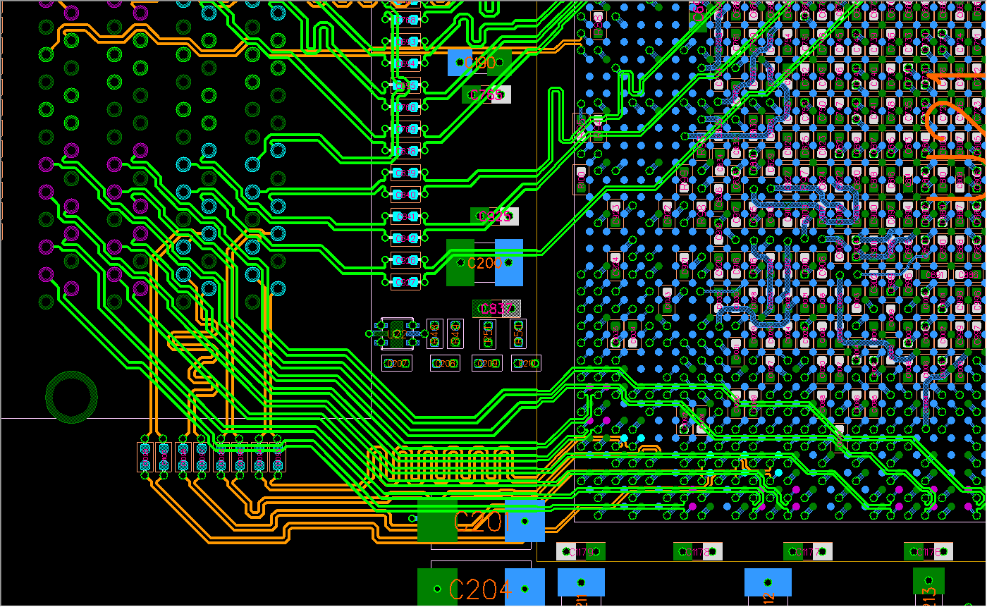
Optimizing Trace Width for Signal Integrity:
Maintaining signal integrity is paramount in high-speed PCB designs. Narrow traces can introduce impedance mismatches and signal distortion. By optimizing trace width and impedance matching techniques, engineers can ensure reliable signal transmission and minimize signal degradation.

Image source: Images are sourced from the internet. If there are any copyright concerns, please contact us for removal. Thank you.
Thermal Management Strategies:
Effective thermal management is crucial for preventing overheating and ensuring the longevity of electronic components. Wider traces facilitate better heat dissipation, reducing the risk of thermal runaway and component failure. Incorporating thermal vias and copper pours can further enhance thermal performance.
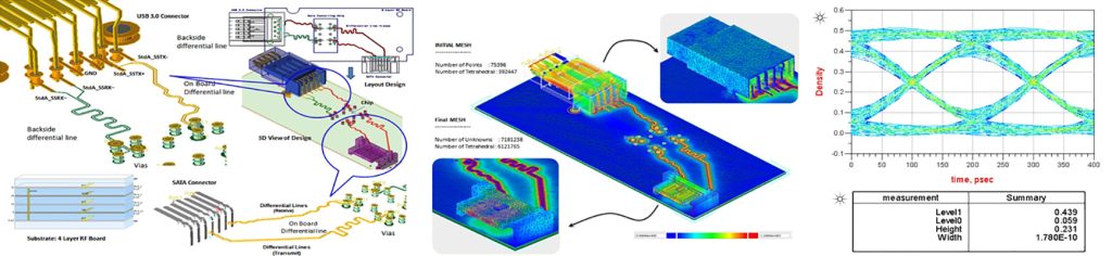
Image source: Images are sourced from the internet. If there are any copyright concerns, please contact us for removal. Thank you.
Advanced Techniques for Trace Width Design:
Advanced techniques such as controlled impedance routing, differential signaling, and impedance matching networks can further improve signal integrity and EMI performance. These techniques require careful consideration of trace width, spacing, and layer stackup.
Image source: Images are sourced from the internet. If there are any copyright concerns, please contact us for removal. Thank you.
Conclusion:
Mastering PCB trace width design is essential for achieving optimal circuit performance and reliability. By understanding the fundamental principles and employing advanced techniques, engineers can design PCBs that meet the stringent requirements of modern electronic systems.