目录
Toggle6 Layer PCB Stackup, Thickness, and Manufacturing: An In-Depth Guide
Understanding 6 Layer PCB
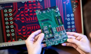
6 Layer PCB are critical in complex electronic systems, offering enhanced capabilities for intricate designs. These boards, made up of six interconnected layers, provide superior electrical performance for demanding applications.
Designing a 6 Layer PCB
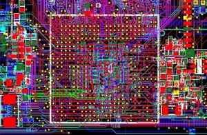
The design phase of a 6 Layer PCB is pivotal. It involves planning for layer arrangement, signal integrity, and thermal management, using advanced software tools for layout and schematic design.
Material Selection in 6 Layer PCBs
Material choice is crucial for 6 Layer PCB. Common materials include FR4 for the substrate, high-quality copper for conducting layers, and specialized dielectrics for insulation and impedance control.
The Manufacturing Journey
Manufacturing a 6 Layer PCB requires precision. It includes processes like lamination, drilling, plating, and etching. Each step is meticulously performed to ensure the integrity and functionality of the final board.
Typical Parameters for 6 Layer PCB
| Parameter | Description |
|---|---|
| Layer Count | 6 |
| Material | Commonly FR4 |
| Board Thickness | Varies, often around 1.6 mm |
| Copper Thickness | Standard 1 oz/ft², adjustable |
| Min. Trace Width | Usually around 0.1 mm |
| Min. Hole Size | Often 0.3 mm |
| Surface Finish | Options like HASL, ENIG |
| Solder Mask | Various color options available |
Diverse Applications of 6 Layer PCBs
6 Layer PCB are used in various sectors, including telecommunications, medical devices, and aerospace, thanks to their ability to support complex circuitry and high-speed data transfer.
Conclusion
6 Layer PCBs are a cornerstone in advanced electronics. They strike a balance between complexity and performance, making them ideal for sophisticated electronic applications.