目录
ToggleCore Strategies in Designing Mixed Signal PCB
Introduction
Designing a mixed-signal PCB layout is a challenging topic, with more complex considerations involved than in pure digital or analog circuitry. This article will cover aspects of component placement, circuit board layering, grounding planes, and dealing with related matters.
Overview of Mixed Signal PCB
A mixed-signal PCB is a type of circuit board that uses both analog and digital signals. These signals run parallel to each other on the circuit board and the design must ensure that they do not interfere with each other for maximum efficiency.
Component Placement in Mixed Signal PCB
The first step in designing a mixed-signal PCB is akin to creating a blueprint for a building. We need a plan for your design. This blueprint will establish the architecture of the entire system design and will aid in mitigating any interference from high noise signals.
As you begin to develop this blueprint, it’s suggested to follow the signal paths on the schematic diagram, particularly for high-speed circuits.
Separating Analog and Digital Modules
To minimize the interaction paths between the analog and digital signals, it’s suggested that the analog part and the digital part be separated to avoid confusion between the analog and digital signals.
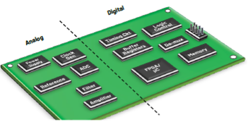
The separation strategy shown in Figure 1 can serve as a reference. When separating the analog and digital parts, keep the following points in mind:
- Sensitive analog components such as amplifiers and nominal voltage sources are recommended to be placed within the analog plane. High noise digital components such as logic controls and timing modules can be placed on another side or the digital plane.
- If a design includes a ADC or a DAC with lower digital current, it can be treated similarly to the analog components.
- For designs with multiple high current ADCs and DACs, it’s recommended to separate the analog and digital power, e.g., associating AVCC with the analog part and DVDD with the digital part.
- Microprocessors and microcontrollers may take up large portions of space and generate heat. We suggest placing such components at the center of the circuit board for optimal heat dissipation and aligning them close to the respective circuit modules that they operate.
Power Module
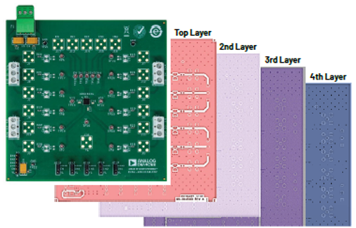
| Layer Position | Layer Type |
|---|---|
| 1 | Digital/Analog signal (Top layer) |
| 2 | Ground |
| 3 | Power plane |
| 4 | Auxiliary signal (Bottom layer) |
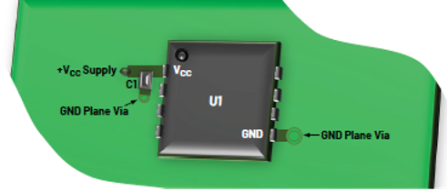
- The power module, the lifeblood of the circuit, must be handled well. A rule of thumb is that the power module must be isolated from the rest of the circuit yet close enough to power the components.
- For components with multiple power pins, we can designate dedicated analog and digital power modules to dampen interference from high noise digital signals.
- Power lines should be short and straightforward, and wide connection lines should be used to reduce inductance and avoid causing current limiting.
Decoupling Technique
- The Power Supply Rejection Ratio (PSRR) must be thoroughly considered in the design process. PSRR reflects the influence of power variance on the performance of components and maintaining a good PSRR is very important.
- Decoupling capacitors can be used to reduce the noise from the power source to the components. Providing the shortest return path for the current is a fundamental principle of proper decoupling.
In conclusion, a good mixed-signal PCB design must take into account various factors such as component placement, separation of analog and digital modules, layout of the power module, and decoupling techniques. Understanding and applying these basic standards can help engineers effectively design and optimize mixed-signal PCB to achieve the best performance in their products.